Tubular Peas
About Nanotubes
Nanotubes, discovered in 1991, are a new form of carbon. With four electrons available for bonding, the carbon atom can combine with others in a number ways and produce many useful materials. For instance, diamond, as shown in the diagram, has each carbon atom bonded to four neighbors in three dimensions, making diamond by far the hardest natural substance found on Earth.
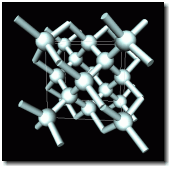
in diamond
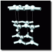
in graphite
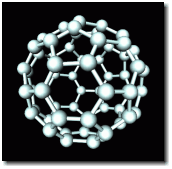
in a buckyball
(images courtesy of
Institut Laue-Langevin, Grenoble)
A much more common form of carbon—graphite—is what we call “lead” in our pencils. Unlike diamond’s three-dimensional structure, the carbon atoms in graphite bind to three others in hexagonal two-dimensional sheets, which slip past each other easily, so the graphite slides off the pencil point and onto the paper. See the diagram for the structure of graphite.
An unexpected new form of carbon, the buckyball, was discovered in 1987, in the soot left behind when a high electric current makes an arc between carbon electrodes. Buckyballs are closed three-dimensional structures, and they are very strong. The diagram shows the simplest buckyball structure, C60.
This same soot from carbon arcs can yield another new form of carbon, the nanotube. As their name suggests, nanotubes are quite small—their diameter is only a few nanometers, less than one ten-thousandth the diameter of a human hair. (More information about the Nanoscale) Nanotubes have been grown up to a millimeter long.
To picture a nanotube, imagine rolling up a sheet of graphite to make a narrow cylinder, as shown in the diagram. Each carbon atom is still bonded to its three nearest neighbors, and this array of bonds makes nanotubes 100 times stronger than steel at only about one sixth the density. Moreover, nanotubes have useful electrical properties that may lead to all sorts of applications.
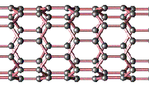
Side view of nanotube showing network of interlocked carbon atoms (Copyright V. H. Crespi. Distributed under the Open Content License.)
Research
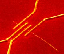
Tungsten leads (bright yellow) deposited to make electrical contact with a nanotube; the contacts are about 80 microns wide; resulting measurements showed some nanotubes are conductors, like copper wire, and others are semiconductors, like silicon, the material of transistors (photo courtesy of Henri Lezec, ISIS, Université Louis Pasteur, Strasbourg France)
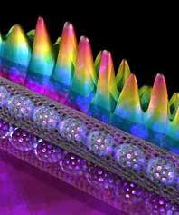
A nanotube filled with buckyballs. The wavy pattern shows the electron density inside the nanotube. (photo courtesy of Ali Yazdani, University of Illinois)
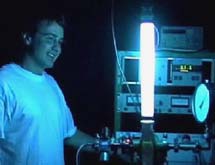
Nanotubes in an electric field spray out electrons. In this experiment, these electrons strike the phosphor coating inside an evacuated glass tube and make it glow, illuminating physicist Olivier Noury. (photo courtesy of Jean-Marc Bonard, École Polytechnique Fédérale de Lausanne)
Nanotubes conduct electricity, but since they’re so small, it’s not easy to attach wires to make electrical measurements. The image shows four electrical contacts deposited over a long nanotube, and the resulting measurements showed that some nanotubes conduct like metals and others like silicon, the material of transistors. In fact, the idea of building transistors and eventually computers out of nanotubes has created a lot of excitement.
Finding a way to control nanotube conductivity has been the focus of much research. One promising approach is to fill the nanotubes with buckyballs—one new form of carbon encapsulated in another to create what is picturesquely termed a “nanoscopic peapod”. (See image.) The number and location of the buckyballs determine the electronic properties of the peapod, an important step on the road to an active electronic device.
Nanotube transistors have in fact been constructed, but they cannot yet be fabricated and connected together in large numbers, nothing like the 50 million transistors on a modern computer processor chip. Nevertheless, nanotubes are leading candidates to replace silicon in the drive to further miniaturize the transistor.
In a different kind of electrical application, when a voltage is applied to a bundle of nanotubes in a vacuum, the nanotubes produce a spray of electrons. If these nanotubes are placed inside a phosphor-coated glass tube and a voltage is applied, the nanotubes give off electrons, which strike the phosphor and make it glow, much like a fluorescent light. The photo shows one of these nanotube lamps. This effect may also lead to a new flat-screen color display for video.
Developing some of these applications can require exacting work with individual nanotubes. When they form in soot, they are part of a tangled mass, as shown in the image on the left. But now nanotubes can be produced in neat arrays, as shown in the image on the right, which could facilitate construction of a device from individual nanotubes. Stay tuned for more news on nano-applications!
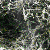
Mat of nanotubes in the soot from a carbon arc discharge (image courtesy Rensselaer Polytechnic Institute)
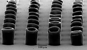
Nanotubes grown in an array (image courtesy of NASA)
Links
Penn State University
Physics World
NASA
Photonics Technology News
Florida State University
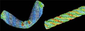
Two nanotubes, one bent (image courtesy of NASA)


